In recent years, with the rapid development of semiconductors, new energy, life sciences, analytical instruments, and high-purity fluid systems, "Ultra High Purity PEEK (UHP PEEK)" has gradually become a focus of industry attention.
Many people believe that high-purity PEEK simply means:
Lower metal content
No additives
Purer raw materials
But in fact, the world's leading companies understand high-purity PEEK far beyond these basics.
For advanced manufacturing industries, materials must not only possess excellent mechanical properties, temperature resistance, and chemical corrosion resistance - more importantly, the material itself must not become a source of contamination.
In traditional industrial applications, PEEK is primarily evaluated based on material performance. However, in semiconductor and high-purity fluid systems, the most critical concern for customers has fundamentally shifted.
The core objective of high-purity PEEK has evolved from "performance enhancement" to "contamination control."
According to international public data, high-purity PEEK primarily addresses three layers of impurities:
Layer 1: Low Metal Ions
One of the most closely monitored contamination sources in the semiconductor industry is metal ions — such as Na, K, Ca, and Fe. Even at extremely low concentrations, these elements can migrate onto wafer or product surfaces during use.
Key achievement of high-purity PEEK:
Sodium (Na) content ≈ 1 ppm
Purified PEEK is currently undergoing continuous testing to address related issues.
Layer 2: Material Extractables
Many materials perform excellently in factory testing, yet after a period of use, they can still cause system contamination. The reason is that residual substances inside the material may gradually leach out in ultra-pure water (UPW), acid solutions, alkaline solutions, and high-temperature environments.
This is why tests such as SEMI F57 and ICP-MS are receiving increasing attention.
Layer 3: Invisible Volatile Compounds
In vacuum, high-temperature, and plasma environments, certain organic residues gradually volatilize:
Forming thin-film contamination
Increasing particle risk
Affecting long-term equipment stability
True high-purity PEEK requires not only low metal ion content but also Low Outgassing.
Many people believe the main difference between high-purity PEEK and standard PEEK lies in testing standards. In reality, the greater difference lies in the manufacturing process.
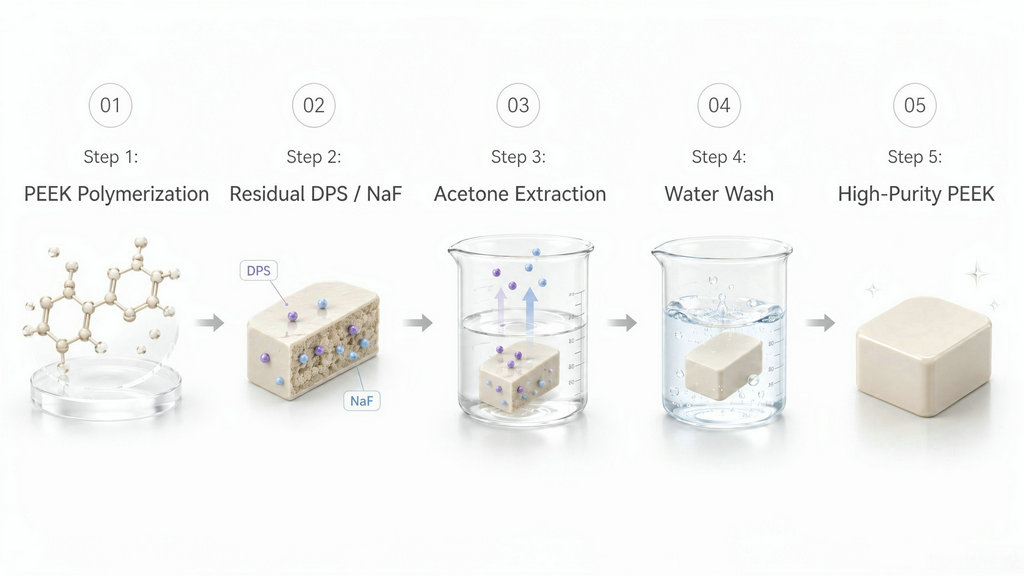
Residuals from the Polymerization Process
PEEK polymerization leaves residual Na⁺ (sodium ions), K⁺ (potassium ions), Ca²⁺ (calcium ions), F⁻ (fluoride ions), volatile impurities, and other elemental impurities. These residuals require additional purification processes to remove.
Purification Steps Include:
Acetone extraction (removing DPS)
Water washing (removing NaF)
Multiple acetone leach cycles
Multiple water leach cycles
These steps systematically reduce residual levels.
Therefore, the cost of high-purity PEEK is not just the resin itself - it is the additional purification cost.
Many materials can achieve very clean surfaces through post-processing and washing. But what truly determines long-term performance is whether the material is equally clean inside.
It is worth noting that even for leading international companies, high-purity PEEK development still faces challenges. Public data shows: Mg levels still reach 9.5 ppm; Ca levels still reach 7 ppm.
With the development of semiconductors, high-purity fluids, new energy, and high-end equipment, customer requirements for PEEK have evolved:
True high-purity PEEK is not just about low metal ions. It is a systematic engineering effort encompassing:
Raw material selection
Polymerization process control
Multi-stage purification
Rigorous testing and validation
Consistent batch-to-batch quality
The competition in high-purity materials has essentially shifted from performance competition to contamination control capability competition.
Copyright © PEEKCHINA | Taizhou Ark International Trade Co.,Ltd. All Rights Reserved |
Sitemap
| Powered by



 EN